Nano. The word rolls off the tongue as if it could be a name for a garage band or a cartoon character. Strange that it should sound so whimsical, this prefix assigned by Le Système international d’unités authorities to designate 10-9. When affixed to units of length, it becomes the nanometer: 0.000000001 meters long.
Tiny? Oh, goodness, tiny doesn’t begin to describe the realities of nano-land.
Even the most infinitesimally small tangible examples are measured in hundreds to thousands of nanometers (nm). Run this page between your fingers; it’s about 250,000 nanometers thick. At 75,000 nanometers, a human hair, while small, is still visible to the naked eye. Think smaller, think cellular. At about 5,000 nanometers, the human red blood cell is invisible without a light microscope; this same microscope has a tough time locating, at 800 nanometers, a dust particle. Far more powerful instruments and techniques are needed to visualize the virus that causes influenza, which is about 100 nanometers wide, or to study the structure of the “molecule of life,” the DNA helix, which is two nanometers wide.
As you can imagine, it’s difficult to detect anything this small let alone manipulate it. Yet, there is good reason to: with only a reduction in size but no change in substance, tiny materials can exhibit new properties—things like electrical conductivity, elasticity, greater strength, different color, and greater reactivity—that they do not exhibit at macroscale, or even microscale. Working at nanoscale, at dimensions between approximately 1 and 100 nanometers, scientists can utilize these unique physical, chemical, mechanical, and optical properties, which are known as quantum effects.
Much of the recent boom in nanotechnology research was driven by development of new instruments in the 1980s like atomic force microscopes, scanning tunneling electron microscopes, and others that allow visualization of nanometer-sized structures. These research tools provide scientists with new pathways to understanding quantum effects and other simple physical effects, such as expanded surface area, that occur naturally when matter is organized at nanoscale.
Take gold, for example. In bulk—that is to say, when all the particles are lumped together—the element is largely unreactive; gold jewelry requires little polishing because it barely oxidizes. Gold nanoparticles, in contrast, are highly reactive, even acting as a catalyst to promote certain types of chemical reactions. In another example, aluminum (like the kind you find in a soft drink can) may spontaneously combust when reduced to nanoparticle size. The form of carbon called graphite is used in pencils because it is soft, yet nanoscale carbon can be stronger than steel and six times lighter. Clearly, common materials reorganized at the nanoscale offer a wide new range of possibilities to researchers.
Scientists are daily learning new ways to isolate and utilize nanoparticles in the emerging field of nanotechnology. Armed with new microscopy techniques, scientists figured out in 1985 how to arrange atoms of carbon into spherical fullerenes—nicknamed “buckyballs” in an homage to Buckminster Fuller, whose geodesic domes they resemble. Carbon nanotubes were discovered in 1991, with applications ranging from electronics to drug delivery. Scientists soon formed carbon molecules into hollow nanospheres, nanoellipses, and other shapes with unique properties. In 2004, a one atom-thick honeycomb-like sheet of carbon atoms called graphene was successfully constructed. With a breaking strength of over two hundred times that of steel, graphene is one of the strongest materials ever tested.
While manufacturing costs remain high and there are other challenges to moving the application of these materials into the private sector, today there are a breathtaking number of ways to leverage nanotechnology. Researchers are developing advanced materials for use in cars, airplanes, construction materials, and consumer goods. With the aid of engineered “smart” nanoparticles, disease-fighting drugs can be delivered to a specific place in the human body in just the right amount. The unique conductive properties of some nanomaterials could be critical to making renewable energy feasible, or could lead to the next advance in computer microprocessing.
Make no mistake about it: just as the development of plastic polymers revolutionized manufacturing and products throughout the second half of the 20th century, nanotechnology will likely impact the next several generations of humans. If human history is measured by our capacity to build better tools, we may be poised on the edge of the Nanotech Age.
To better understand the promises and problems of nanotechnology, Wisconsin People & Ideas interviewed four professors in the University of Wisconsin System: Drs. Michael Zach (UW–Stevens Point), Robert Hamers (UW–Madison), James Hamilton (UW–Platteville), and Pradeep Rohatgi (UW–Milwaukee). Each professor has devoted his career to nanoscience research, and each approaches it with a different perspective. Their stories and thoughts are provocative, intriguing, and surprising—not unlike the field of nanotechnology itself.
• • • • •
Michael Zach is assistant professor of chemistry at UW–Stevens Point. His research could be described as “low-tech high tech” since he and his research group have developed ways to make patterned nanowires without the need for expensive, equipment-laden clean rooms typically used for making computer chips. The process involves nanoscale electroplating, where a template is made on which to pattern the deposition of nanowires. Described as “a real Renaissance man” by collaborator James Hamilton (also profiled in this article), Zach’s path to nanoscience research included several years as an artist, jeweler, and gemologist. He even served as a jeweler and sculptor apprentice to a religious monk in Florence, Italy. After completing his MS and PhD at the University of California–Irvine and postdoctoral research at UC–Berkeley and Argonne National Laboratory, Zach returned to his undergraduate alma mater to teach and conduct research.
What led you to this “low-tech high tech” area of nanotechnology research?
My interest is in developing technology that is accessible to more people by working in nanotechnology. We need to figure out a way to make things smaller in a much more economical way. … What drew me to [this area] was the ability to make high-tech structures that are normally in the realm of what’s done with electron beam lithography or that require very tedious, expensive lithography to make, and instead being able to do it on a normal laboratory bench top [using chemical solutions kept in] “baby food-like” jars. It’s something that captures the imagination of undergraduates and gets them thinking about how they can apply what they’re learning in the classroom and encourages them to make discoveries.
In general, it sounds like there is a wide range of nanodevices or nanotechnology-enhanced materials that could be within reach in the future.
Sure. Imagine someday having particles or complete little circuits that are so small you could put them into plastics. Let’s say those circuits are little RFID [radio frequency identification] tags which can be put into a polymer; as that polymer nears the end of its life and cracks are starting to form, the signal changes and says, Hey, I’m a part [that is] in danger of failing. I need to be replaced.
Say you’re on a manufacturing floor and there are two parts that someone is trying to assemble. You could have these two parts talking back and forth to each other [to ensure they are assembled correctly]. Medical devices could be designed to have diagnostics built in [RFID] tags could be put into the paper used to make currency so even if a counterfeiter tried soak off the dye, to change $1 bills into $20 bills, there’s still a signal emanating from the paper saying, I’m a $1 bill.
There are all sorts of different types of smart materials that can be developed, but we have to work toward the complexity of these types of devices.
Is this the kind of manufacturing that could benefit, say, developing nations?
Eventually my hope is that we can create a technology that can be done without all of the fancy tools. In some respects, we have our own third world country right here within the United States: It’s called rural America. We need to create high-tech industries that can be done in small mom-and-pop start-ups. What we’re doing [in my lab] is to develop a scenario such that once the electrodes are made, nanomanufacturing can be performed just about anywhere. Instead of having to invest in a multi-million dollar clean room, you could perform nanomanufacturing for much, much less than $10,000. Bringing the wealth of good quality manufacturing to non-traditional areas for high-tech manufacturing will help raise the region’s economy.
With professional experience as an artist, a goldsmith, and as a photographer, do you find this research to be aesthetically appealing?
Absolutely. I approach nanotechnology by drawing from ideas that I developed as a jeweler, or even as a seven-year-old kid walking home through the fields. I draw from all different aspects of my life experience. Looking at these various samples using the electron microscope or with an atomic force microscope, there’s always surprising beauty and simplicity. For example, a bismuth wire has these beautiful little facets and crevices at periodic or semi-periodic intervals. I ask myself, Are those semi-regular voids able to be used in a way that I never envisioned? Little aesthetic surprises [like these] keep me thinking about the structures.
Sounds like a good approach. What can we do to get students excited about science or encourage them to become more involved in science-based careers?
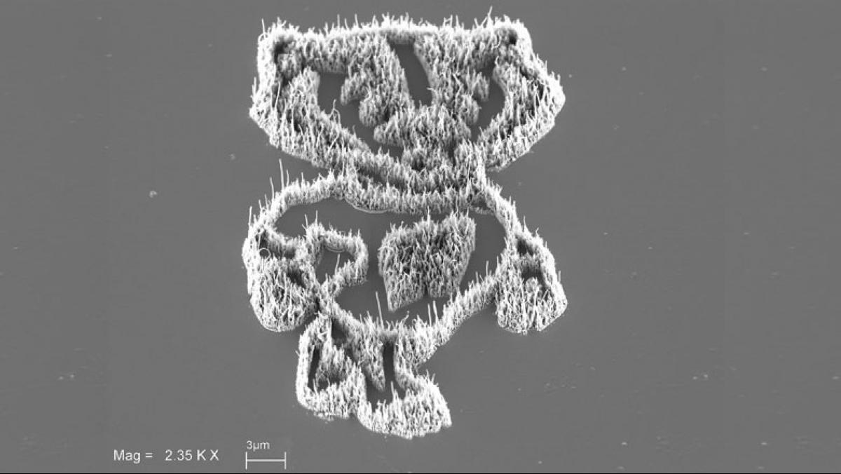
Last year I won honorable mention in the NSF and Science magazine’s International Science and Engineering Visualization Challenge for a project that involves geology, chemistry, biology, and microscopy all in one. The image [from the project] is an example that I use in teaching to get students thinking about how they can combine several different disciplines to solve really tough problems.
When I graduated I didn’t realize the number of opportunities out there for a scientist. If you would have told me when I was an undergraduate that I’d have the cover of Science magazine or that I’d be teaching at one of the top schools in the nation, I wouldn’t have believed you—not based on my background, coming from a town with 10,000 people and 40,000 cows. There aren’t a lot of role models for scientists in these smaller towns, other than the family doctor. I see it all the time with my students coming from small rural farm towns, extremely bright students and they just don’t know what opportunities exist or where to apply their newly learned skills for making a difference in the world. So that’s kind of why I’m here at Stevens Point.
• • • • •
Robert Hamers is the Arthur Adamson Professor of Chemistry at UW–Madison and has been designated a Wisconsin Distinguished Professor by the University of Wisconsin System. During his seventeen years at UW–Madison, Hamers has built a large and dynamic research laboratory focusing on such subjects as semiconductor surface chemistry and nanoscale molecular architecture. In addition to mentoring dozens of postdoctoral scholars, graduate students, and undergraduates, he regularly advises middle school and high school students performing research internships in his laboratory. Hamers also holds leadership positions at the UW–Madison Nanoscale Science and Engineering Center (NSEC) and the UW–Madison Materials Research Science and Engineering Center (MRSEC). With over 230 research articles and eleven issued U.S. patents, Hamers is one of the most highly cited scientists in the field of Materials Science. He serves on a Wisconsin State Legislative Special Committee on Nanotechnology, and in 2009 testified during an informational hearing of the Wisconsin State Assembly Committee on Public Health on Applications and Environmental Impact of Nanoscale Materials.
You have an incredibly deep and broad research program. Could you briefly describe your main areas of research?
Most of my research focuses on surfaces of materials. To a first approximation I’d be described as a surface scientist or surface chemist, in the sense that my area of expertise is primarily in understanding the unique features of surfaces of materials and designing strategies for designing, controlling, and manipulating surface chemical and electrochemical processes. This becomes important in nanoscale materials. As the material becomes very small, the fraction of the atoms that are present at the surface versus being buried in the bulk increases dramatically. Surfaces begin to dominate the physical as well as the chemical properties of the material. That high surface-to-volume ratio is being taken advantage of increasingly in a number of areas relating to renewable energy. Examples include new kinds of solar cells or photovoltaic devices [which convert light to electricity at an atomic level] that take advantage of the high surface area of materials to transfer electrons.
Also, I do a fair bit of work in next-generation lithium ion batteries [and energy storage]. There, also, the electrical performance depends very heavily on the microscopic structure of the materials. We investigate those materials and the surface reactions that occur. (Just to be clear, I have a small company that I started three years ago focusing on the next-generation lithium ion batteries.)
Could you comment on what motivates you and excites you most about nanomaterials? What are some of the most compelling aspects of this research?
Right now I think the most compelling reason for wanting to investigate nanomaterials evolves from the fact that nanomaterials are probably key to solving many of the energy problems that we face today. The use of nanoscale materials is leading to new … low-cost, energy-efficient devices for converting solar energy into electrical energy, for example, [as well as to] advances in energy storage. Many advances in renewable energy, especially photovoltaic devices, revolve around controlling nanoscale structure of materials.
Probably an even bigger challenge as we move forward is not making energy, but storing energy. All solar conversion devices and wind farms ultimately rely on daily fluctuations in the solar cycle and in the daily cycle of wind. Yet we want to be able to use energy twenty-four hours a day, seven days a week. So, it becomes increasingly important to develop means for storing energy. We also see storage needs emerging as we make electric vehicles, for example. Many of these hinge on the ability to make energy storage devices, such as batteries, with very high performance. That high performance comes from the use of nanoscale materials.
Aside from the inherent realities of trends in funding and fundability, how do you and those in your lab choose which research problems to pursue next?
I like to look at areas where I think there will be revolutions in technology, or there could be revolutions in technology, fifteen to twenty years down the road. And then I like to pull back from that two steps, and try to address the fundamental science limitations that currently make those technologies impossible. … With a lot of technologies, if you’re looking at things that are only five years away from fruition, you’re really focusing on [fine-tuning] and engineering. But if you’re looking at things that are fifteen to twenty years away, there’s greater room for creativity. … I like to be able to look at problems where there isn’t necessarily a known solution—yet—or where there may be many solutions, and try to say, What are the fundamental scientific questions that need to be answered? In particular since our emphasis tends to be on surfaces, chemical reactions of surfaces, and electrical properties of materials, where are the areas where our unique expertise can be brought to the problem in a way that might constructively lead to solutions on that kind of a time scale?
What are some of the biggest problems in the field right now?
A big question revolving around nanomaterials is understanding the environmental safety and health impacts associated with the use of nanomaterials. We like to use nanomaterials in these various emerging applications because of the fact that nanomaterials have unique properties. And for the most part, we think that these properties can be beneficial. However, there is also concern. For example, because nanoparticles are so small—much smaller than the size of a human cell—nanomaterials may have some inherent risks associated with their use. And it’s really important that we understand what those risks are, and that we’re able to perform a real risk-benefit analysis. [Editor’s Note: Federal research dedicated to nano-related environment, health, and safety issues grew substantially from $35 million in FY 2005 to an estimated $117 million requested for FY 2011. Between FY 2005 and FY 2011 the National Nanotechnology Initiative will have invested $484 million in research with the primary function of understanding the impact of nanotechnology on our environment, health, and safety].
That’s a good segue into the topic of nanotoxicity. I noticed your 2009 paper on the zebrafish embryo as a model of nanotoxicity in the environment. Do you feel that the tools are in place to assess some of the nanotoxicity and environmental impact questions, or are there additional models that need to be developed in tandem with these new nanomaterials?
There’s an enormous amount of work that needs to be done. [Recently] I co-organized a two and a half day workshop in Arlington, Virginia, for the National Science Foundation that focused very much along the lines of your question: How do we understand the environmental health and safety impacts of nanomaterials? Where are the gaps in our knowledge? Where do we lack the tools and abilities to measure things, and what should we be doing as scientists to try to address those problems?
So, there are a lot of really complicated challenges. One of the biggest challenges in nanomaterials is that, for example, if [you] make a lithium ion battery, this lithium ion battery will probably have in it some nanoscale metal oxides, like lithium cobalt oxide. These materials, if they are released into the environment—suppose someone throws the battery into a landfill instead of recycling it—undergo a series of chemical and physical changes that can occur over a very long time scale. So one of the challenges in trying to assess the environmental impact of nanomaterials is that they’re not constant. They’re changing. They’ll start off as an engineered particle with a precisely defined structure and composition that was chosen because of the application of the materials. But they can be modified by the environment, and they will also induce changes in the environment. And these changes occur on a range of scales. For example, the interactions of nanoparticles with cells, with naturally occurring organic matter, could potentially lead to … the concentration of nanoparticles [within a living plant or animal].
You have a long-standing interest in astronomy and also amateur radio work, yes? There is a fascinating juxtaposition when you consider the impossibly macro scale of celestial bodies in comparison to nanoscale materials. Do you find any intellectual interplay between those two areas?
All the time. Understanding astronomy and understanding how a telescope works, for example, teaches you about optics, which is at the heart of most instruments that are used in nanotechnology. But really it comes back to, I think, getting excited about science.
I grew up in the 1960s, and like many kids of my era, this was a time [to be excited about] the Apollo program. And the astronomy bug comes from the fact that my grandfather, who was a machinist by training, got a metal lathe when he retired and he learned how to grind mirrors. He made this enormous telescope that was the length of his garage. In order to look into it, I had to stand on top of a very tall ladder. But as a kid, it allowed me to get a different view of the universe. We would roll this telescope out into a very dark alley next to his house and look at the stars, the moon. And you know, that was a time when science was cool. It was really great to be a scientist. That’s what sparked my interest in having a scientific career. And that has persisted to this day.
• • • • •
James (Jim) Hamilton is a Professor of Physical and Analytical Chemistry at UW–Platteville, and has founded two companies: Photonic Cleaning Technologies, which develops, manufactures, and sells specialized polymers for cleaning optical surfaces; and Xolve (formerly named Graphene Solutions Inc.), which develops nanomaterials and solvent-solubilized nanomaterial systems. Hamilton’s eclectic research interests have led to collaborations with research groups in Ireland and Norway as well as here in the U.S. at the W.M. Keck Observatory in Hawaii, Argonne National Laboratory, and the Smithsonian Museum of Natural History. In 2004, his research group was asked by the Smithsonian Institute to use technology developed by Hamilton to clean the world-famous Hope Diamond.
What are your main areas of nanotechnology research?
We study fundamental properties and thermodynamics of nanomaterial solutions. We try to convert this information into useful applications and products. We’re working primarily in three areas: energy systems and energy storage, coatings and photovoltaics, and composite materials. We span a very wide range of different areas because the discoveries that we’ve made are so fundamental that they’ve really changed the game. We’re making better lithium ion batteries and also capacitors; we can make better coatings for optics and catalysts, and photovoltaics in solar cells; and [we can also] make stronger and better plastics and composite materials. So we’re really able to harness the true strength and flexibility of nanomaterials.
I understand that you’ve commercialized some of these technologies by starting two companies, Graphene Solutions—now known as Xolve—and Photonic Cleaning Technologies.
Yes, Xolve, it’s pronounced like ex-solve. We use the term as a verb. Xolve started out with [research on] carbon nanotubes, which have one thousand times the conductivity of copper and one hundred times the strength of steel, and they conduct electricity a hundred times faster than silicon—as does graphene.
What’s held back the application of nanomaterials since the early 1990s, particularly with carbon nanotubes, is that all of these things tend to clump in bundles. They like each other more than they like any other materials, so they’re difficult to separate.
When [the nanotubes] are in their individualized state, you can really take advantage of their super-properties. They are the quintessentially insoluble materials on the planet; [however] they can’t be used very readily in [an insoluble] form. What we discovered was that there existed certain specific solvent blends that could dissolve these things and exfoliate them into their individual components. And then we discovered—this was a fundamental new principle in nanomaterials—that not only do nanotubes do this, [but also] graphene, which was quite a big deal. We were even in Scientific American magazine for this discovery. Then we discovered that [this dissolving and exfoliating process] holds for a lot of other materials also: many metal oxides and other things that are used in batteries and solar cells. So we’re doing a lot of research on that.
Photonic Cleaning Technologies, your other company, is more mature, correct? With products on the market in a number of countries?
Photonic Cleaning Technologies manufactures some polymer solutions that are used to protect and clean precision surfaces. That’s been around for a little while and it’s growing steadily. … What we developed is the technology of taking liquid polymers and spraying or painting them on the surfaces. They dry to a Saran-wrap-like film. And then when they are peeled off after drying they take off all the junk from the surface, leaving no residue and leaving the surface truly atomically clean. It’s been used by NASA and others. … It’s a very exciting industry and field to be in.
Earlier in your career you had some other life experiences: K–12 teaching, running a painting business, even working on an oil rig. Have those types of experiences informed your approach to commercializing the technologies from your research?
I think so. Everything—from working on a farm when I was in high school and beginning college to having a painting company and then working in the lab—has enabled me to kind of be a jack of all trades. So in our laboratories, and in my work, I was never afraid to do anything. We build our own equipment. We didn’t necessarily rely on buying it because it’s extremely expensive. And when I was at UW–Madison I learned to build instrumentation and do really world-class research with a big group. And it just kept going from there.
You’ve talked a little bit about what drew you to the discovery of polymer optical cleaning applications. But, in terms of Xolve, did you have an application in mind when you began experimenting with different ways to solubilize graphene or was it more of a basic research question motivating you?
That’s a great question. The success of Xolve is really a wonderful story of serendipity and time, and the true beauty of following the scientific method. Because it was absolutely pure research, with no applications in mind.
We had just published a paper where we had taken carbon nanotubes and incorporated them into the polymer First Contact, and it made the polymer conductive, so that it would dissipate electrostatic charge and not develop static as you pulled it off. And working with Fermilab and Lawrence Berkeley National Lab on astronomical camera sensors that were going into a telescope in Chile, we were able to clean these sensors, which everyone always assumed would be just impossible. It was a really wonderful result.
[Research on] carbon nanotubes [was exploding], they were being put in all kinds of polymers. Most of the time [the nanomaterials] didn’t really become very conductive. And it just accidentally happened that the polymers that I had developed and worked with for Photonic Cleaning seemed to work well. And we wanted to understand why. And so [a student named] Philip Streich … came to me when he was fifteen and said, “Dr. Hamilton, I’m taking on a science fair project, do you have any ideas?” And so I had just come from Ireland where I was talking about this with my colleague and collaborators over there, Johnny Colman at Trinity College in Dublin. We were trying to understand what was happening with these nanotubes. So Philip and I embarked on a quest to measure the fundamental thermodynamic solubility of nanotubes in these special solvents.
It was … pure thermodynamics. It was as far from applications as you could get. … We built our own instruments and were able to measure and prove that these carbon nanotubes were actually thermodynamically soluble and dispersed and exfoliated in this special solvent mixture, and we didn’t know why that was until we did some molecular modeling. We just kept poking at it and we made these huge fundamental discoveries.
It all started because we were doing some basic research, with no application in mind other than trying to understand some science.
What is the key to successful collaborations like those you’ve had that span such a large spectrum of fields, including astronomy, biology, forensics, and engineering?
I think that the saying, “Luck favors the prepared mind,” is really a key thing. Being around and making friends with other scientists and engineers around the world, having deep and lasting relationships—both professional and personal—it’s really been one of the most crucial events. I think that one of the hardest things is that … I absolutely have too many projects and I’m not focused enough, by normal standards. And that’s an issue. … The key thing has really been to be in the right place at the right time, and going out to meet people, getting out there and starting a bunch of these collaborations—some of which [quickly] lead to things, some of which lead to things ten years down the road.
I think one of the great benefits is that I’ve had the really wonderful support of the administration here in Platteville, where it’s possible to do this. The advice that I would get from other science faculty around the country would be to pick one of these [research areas] and become the international best at it. And an alternative model is what we do: we collaborate and help people, and we have lots and lots of instrumentation that we build and work on. So we’re pretty good at a lot of things, but we’re not the best in the world at anything.
Looking at the breadth of what you’ve done, though, the impact that you’ve had is really tremendous.
Yeah, I’m having trouble getting my head around it. But without question, I still hear in my head the advice of my PhD committee and advisors at UW–Madison in Chemistry who were great mentors. They would say, “Jim, you have to focus. You have to be more detailed about this. Don’t go off all half-cocked.” I never listened. [laughs] And it didn’t kill me.
• • • • •
A Distinguished Professor at UW–Milwaukee as well as director of the UWM Center for Composite Materials and the UWM Center for Advanced Materials Manufacturing, Pradeep Rohatgi has focused on materials science throughout his career. An expert in foundry manufacturing techniques, he performed his graduate work at Massachusetts Institute of Technology, then returned to India to establish and direct two national laboratories: the National Institute of Interdisciplinary Science and Technology in Trivandrum and the Advanced Materials and Processes Research Institute in Bhopal. While in Bhopal, Rohatgi survived one of the worst industrial accidents in history on December 2 and 3, 1984, when a storage tank ruptured at pesticide manufacturing factory owned by the Union Carbide Company. The ruptured tank released the toxic gas methyl isocyanate into the city of 900,000 people, killing several thousand individuals and injuring tends of thousands more. Escaping unharmed, Rohatgi participated in post-accident assessment and advising on alternative disposal of a second tank of methyl isocyanide at the factory site. Rohatgi later joined UW–Milwaukee as a professor and continued his preeminent research on composite materials, particularly metal matrix composites (defined as materials with at least two different constituents, one of which is a metal). He holds sixteen issued U.S. patents, has published nearly three hundred research articles, and has received over $10M in research funding from industry, federal agencies, and the U.S. military.
Could you tell a little about your scientific background, your training both here and in India and later in the U.S., and what it was from that background that drew you to this line of research?
I did my undergraduate work in metallurgy in India. I came to the U.S. and did my doctorate at MIT. I was trained in the field of solidification, which is the basis of the foundry industry. [Editor’s Note: While ice forming on a lake in winter reflects the solidification process—the transformation of a liquid to a solid—the creation of solders for use in electronic circuits or the controlled casting of steel are two common industrial applications of solidification science.]
Right from that time I was very interested in synthesizing new materials, advanced materials, using low-cost foundry and solidification processes. So that’s what got me started. … It is that work that I have continued through my work in industry in the U.S. at the International Nickel Company, the labs where I first synthesized foundry-producible cast metal composites way back in 1966.
Then, I worked for Bethlehem Steel Research Labs on large-scale steel castings, improving their performance. And then I returned to India where I was a professor at the Indian Institute of Technology and the Indian Institute of Science, where I trained a large number of students to synthesize metal matrix composites using solidification processing.
After that, the government of India wanted me to serve as the founder, director, and CEO of two large national laboratories—one in Trivandrum and the second one in Bhopal for the Council of Scientific Research in India. These labs were focused on developing new materials that were needed by society and very often were based on local resources. …
My last job in India was setting up this large laboratory in the city of Bhopal. You may remember that this is the city where the largest industrial accident took place, and six thousand people died. I was head of the national laboratory in this city, and fortunately I survived.
After Bhopal, I moved to Milwaukee, joined the University of Wisconsin–Milwaukee, and developed this research program. It was very much tied to helping local industries in Wisconsin, especially local foundries, to manufacture these very advanced [metal matrix composites], and then stimulating local industries like the automotive industry and small engine industry in Wisconsin to try to use these materials to become more competitive.
So I established the UW–M Composite Center, UW–M Foundry Laboratory, and UW–M Tribology Laboratory to study these materials. [Editor’s Note: Tribology is the study of friction, wear, lubrication, and the design of bearings; the science of interacting surfaces in relative motion.] And then, a lot of industries across the U.S., including Ford, General Motors, Chrysler, Briggs and Stratton, Electric Power Research Institute, National Science Foundation, Department of Energy, [and] the Office of Naval Research. … funded my research very generously, allowing me to develop these new advanced materials and the processes to manufacture them. And in addition to working for transportation and the electric power research industry, we are in fact now working for G.E. Healthcare, trying to develop ultralight materials with very high conductive properties for their CAT scan and x-ray equipment. ...
I’ve always tried to respond to the needs of local industry, and of society. … That’s why a lot of my work has been directed to develop foundry-based manufacturing processes, because Wisconsin is home to the largest number of foundries in the United States at this time.
I am one of those people who strongly believes that any society needs a very strong manufacturing industrial base to remain competitive. I’m very concerned that we are losing a lot of our manufacturing to other countries, and I believe that one way to bring that kind of manufacturing back to the U.S. is to learn to manufacture very high-technology materials of the kind that I am developing. These materials can be made in the U.S. competitively, and it will allow manufacturing to remain in the United States.
Can you give us an overview of your research program in general, and also of your work on nanocomposites and metal matrix composites that have nanostructures within them?
I started the UW–Milwaukee Center for Composites, as well as a new center that was established last year, the Center for Advanced Materials Manufacture. Our objectives are to try to synthesize new materials and develop manufacturing processes so that these materials can be used by industries in the United States—especially in Wisconsin—to improve the competitiveness of U.S. industry.
For a large number of years we have been working on metal matrix microcomposites and metal matrix syntactic foams [Editor’s Note: These foams incorporate hollow particles in a matrix, where enclosing porosity inside the thin shell of the particle leads to low density without large decreases in mechanical properties.] These materials can be very light, and they can save a lot of energy in transportation systems. We have also worked on utilizing for composite materials waste products like fly ash and waste foundry sands, and we have incorporated metallic materials like aluminum and magnesium to reduce the energy content of [composite] metals and to make them much lighter. We have also worked on solving the problem of lead contamination in drinking water by developing lead-free plumbing fixtures for plumbing and building applications.
In recent years, we have tried to direct our work to nanostructured metallic materials, as well as nanocomposites. The reason for moving to nanostructured materials and nanocomposites is that they can be much stronger than conventional microstructured materials or microcomposites. So they will allow you to use much less material, or the component can be much lighter compared to conventional components. So when you use them in [automobile, aircraft, or rail] transportation systems or other applications, you could have tremendous savings in energy.
What are some applications of these materials?
Our focus has been to not only dream of, or synthesize, new materials, but to also develop low-cost mass manufacture processes to make them in mass quantities—particularly in industries in the U.S. and in Wisconsin—using existing manufacturing infrastructure. That’s why one of our focuses has been on using conventional foundry processes [and] conventional metal casting processes …
A lot of our work has been sponsored in the past by automotive companies, and more recently by the U.S. Army because they are interested in reducing the [overall] weight of transportation systems as well as trying to reduce the weight of the military vehicles in the battlefield. We have also extended our capabilities to synthesize new materials like syntactic foams for high-energy absorption materials for use in automobiles in case of an accident.
We have also developed materials that are self-lubricating, so the … energy loss in transportation systems, including automobiles, will be decreased. In the battlefield if your tank has been hit and you have lost oil, the engine will not seize but will continue to run because our pistons and liners are self-lubricating through the incorporation of components like graphite or carbon, including carbon nanotubes.
We are also working in the area of self-healing materials. … So if there is a crack in the material, instead of failing the material will be partly or fully healed and you can recover the original strength of the material despite [presence of] a crack. ... We’re trying to mimic what happens in biological systems in synthetic materials like metal and polymers and ceramics. … [Editor’s Note: This self-healing process occurs after hollow microtubule balloons injected into the material’s metal matrix rupture, releasing a healing agent that interacts with a catalyst and seals the crack like glue.]
We are also beginning to work on self-cleaning materials [that don’t allow] dust accumulation on glass surfaces. You can also reduce the formation of ice on airplane wings, so you don’t need de-icing. There are a lot of applications for this self-cleaning material. You won’t even have to clean the sink in your kitchens and bathrooms because the materials will be self cleaning.
We’re trying to use nanotechnology and nanostructured materials to try to develop stronger materials, materials which are high in conductivity, materials which have special properties including self healing and self cleaning.
All of this is very exciting, but it reminds me that there is a tendency in science journalism to occasionally over-sell or over-promise. We as humans are very optimistic. Do you think that there are any aspects of nanotechnology or nanocomposites that may have been over-promised?
I think that the ideas for large-scale use still remain. But the cost of these nanomaterials—the ability to handle them and incorporate them into large structures at low costs—will slow down adaptation.
The other concern is that these nano-sized particles could do harm to human health. There is a lot of concern and studies on what is the impact of inhaling carbon nanotubes. In my lab, I have not allowed my students to work on carbon nanotubes for this reason. We’re concerned about the health aspects. This may be also a little bit of a decelerator for their use, and I’m pretty sure people will figure out ways to encapsulate them in matrices so they will not be floating around the air to do harm. People will develop techniques so that you can make the nanotubes in situ, inside the matrix itself, rather than adding the powder to metals. Instead, I just make them inside of the matrix materials, so I don’t have to handle any nanomaterials.
So, high cost of materials, difficulty in handling them, difficulty in dispersing them: these are the barriers that scientists will have to face. And these are the reasons that there may be a time gap before they are mass-manufactured.
And then there are issues about how will you recycle a nanocomposite material? What will happen to the recycling stream? These are other concerns that will have to be addressed as this industry grows.
I hear your concerns about safety throughout the lifecycle, from the manufacturing process all the way down. Thinking back to the industrial accident that you survived back in India, did that experience at all shape your ideas about manufacturing safety?
Yes. …You could see that when you put a very high-technology manufacturing industry in a very low-technology environment—and that described India at that time—it can do a lot of damage. I became all the more concerned about environmental impacts of technology. And that is why, after that, I have been all the more concerned about using renewable resources, trying to use waste byproducts, and trying to see how my work can solve environmental problems. So yes, that experience did sharpen my interest. … And therefore, if I have a choice to work on something that has an impact on the environment and safety, I take that on as a research problem over a problem that just drives my curiosity.
Any stories that really come to mind that illustrate the essence of what this research can do?
When I first discovered how to produce advanced composites by simple foundry techniques, I was responding to what you could describe as a dream from industry. I always like to challenge an industry to give me their wish list, give me their dreams. And then I try to see if I can develop materials to meet their dreams.
About forty years ago I was talking to somebody at General Motors, and he was telling me that he likes to use cast iron, which is a commercial material for automobiles, but he wished it could be as light as aluminum. Cast iron has graphite in it, too, and he said, “I wish I could get a much lighter material like cast iron … with the density of aluminum.” And at that time when you went to the textbooks, they told you could not combine aluminum and graphite, based on thermodynamics.
So he gave me a challenge that was heretofore considered as something that was not possible. I love to take on challenges that people indicate are not likely to succeed. And most of the time, I also don’t succeed; but there is a one out of one hundred chance that I do succeed.
One of the messages that I would like to leave is to at least listen to the wish list and the dreams of industries that are looking for new materials.
And the second message is that, when I started working on foundry processes, people told me that it would never be possible to produce certain materials because of a lack of uniformity and so on. These concerns were valid, but people did find ways to get around them. So the other message is, don’t be discouraged if somebody says that it is not likely to succeed. Remain persistent. If not you, then somebody will find a way.
I’ll give you an example. Right now I am trying to build self-healing metals. Many of my postdocs and my graduate students and many industry people tell me it’s a pipe dream, it will never become a reality. But I’m not giving up. There is something inside me that tells me it will be difficult, it will be far away, but it is not impossible.
So that is my message. Try to respond to these dreams that don’t sound possible today, and listen to the warnings, but don’t be stopped by them. Don’t be stopped by naysayers.
And for me … I enjoy research. For me, it’s really not work. I love to stimulate a large number of young people to recognize that discovering something is really fun. It is not work. I [would] like to see more young people, particularly in the U.S., go into research. It is very unfortunate that we have somewhere failed [to attract more U.S. students into research, science, and engineering]. We rely on people coming from other countries to do research here. That needs to change.